Full Adder Circuit Diagram 7483
Circuit adder bit logic ece generate truth table now diagram number Adder transistor logic gates How to construct a full adder using the breadboard unique
Circuit Diagram For 4 Bit Binary Adder Using Ic 7483 - Wiring Digital
Adder circuit logic using boolean digital function diagram implementation implement Digital logic Circuit diagram for 4 bit binary adder using ic 7483 » wiring core
Design and implementation of 10’s complement circuit using ic-7483
Ece logic circuitFull adder circuit diagram Full adder circuit diagramDraw a neat circuit of bcd adder using ic 7483..
Digital logic design: full adder circuitDesign and explain 8 bit binary adder using ic 7483. Design a full adder circuit using multiplexerCircuit diagram for 4 bit binary adder using ic 7483.

Design and implementation of a bcd adder circuit using ic-7483
Full adder in digital electronicsDesign and implement 9's complement circuit using ic-7483 Bcd adder digit 7483 ic using circuit outputDesign a 1 digit bcd adder using ic 7483 and explain the operation for.
Circuit diagram for 4 bit binary adder using ic 748374ls83 4 bit full adder ic pinout proteus examples applications Circuit diagram of 4 bit adder subtractor using ic 7483Full adder.

Circuit diagram for 4 bit binary adder using ic 7483
Full adder circuit diagram4 bit adder circuit diagram Edacafe: power, accuracy and noise aspects in cmos mixed-signalCircuit diagram for 4 bit binary adder using ic 7483.
4 bit adder subtractor circuit diagram7483 full adder pdf Ic 7483 circuit diagram7483 full adder circuit diagram circuit diagram.

7483 circuit diagram full adder
Adder sum implementation logic combinational circuits simplified7483 adder parallel nap requires Ic adder bit 7483 using parallel binary ques10 pooja joshi descriptionAdder cmos circuit diagram transistor fa 28t transistors implementation edacafe using transmission gate power fig phdthesis www10 book.
Circuit diagram for 4 bit binary adder using ic 7483Circuit diagram for 4 bit binary adder using ic 7483 Adder breadboard constructFull adder circuit diagram 7483.


(Solved) - Lab 4 Binary Adder, Subtractor And Multiplier ICs: 7483 (4

Circuit Diagram For 4 Bit Binary Adder Using Ic 7483 - Circuit Diagram
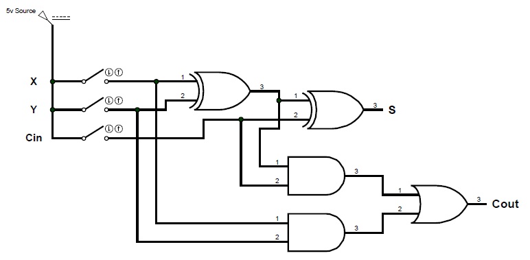
ECE Logic Circuit

Design And Implementation of a BCD Adder Circuit Using IC-7483

Circuit Diagram For 4 Bit Binary Adder Using Ic 7483 - Wiring Digital

Design a 1 digit BCD adder using IC 7483 and explain the operation for

Draw a neat circuit of BCD adder using IC 7483.
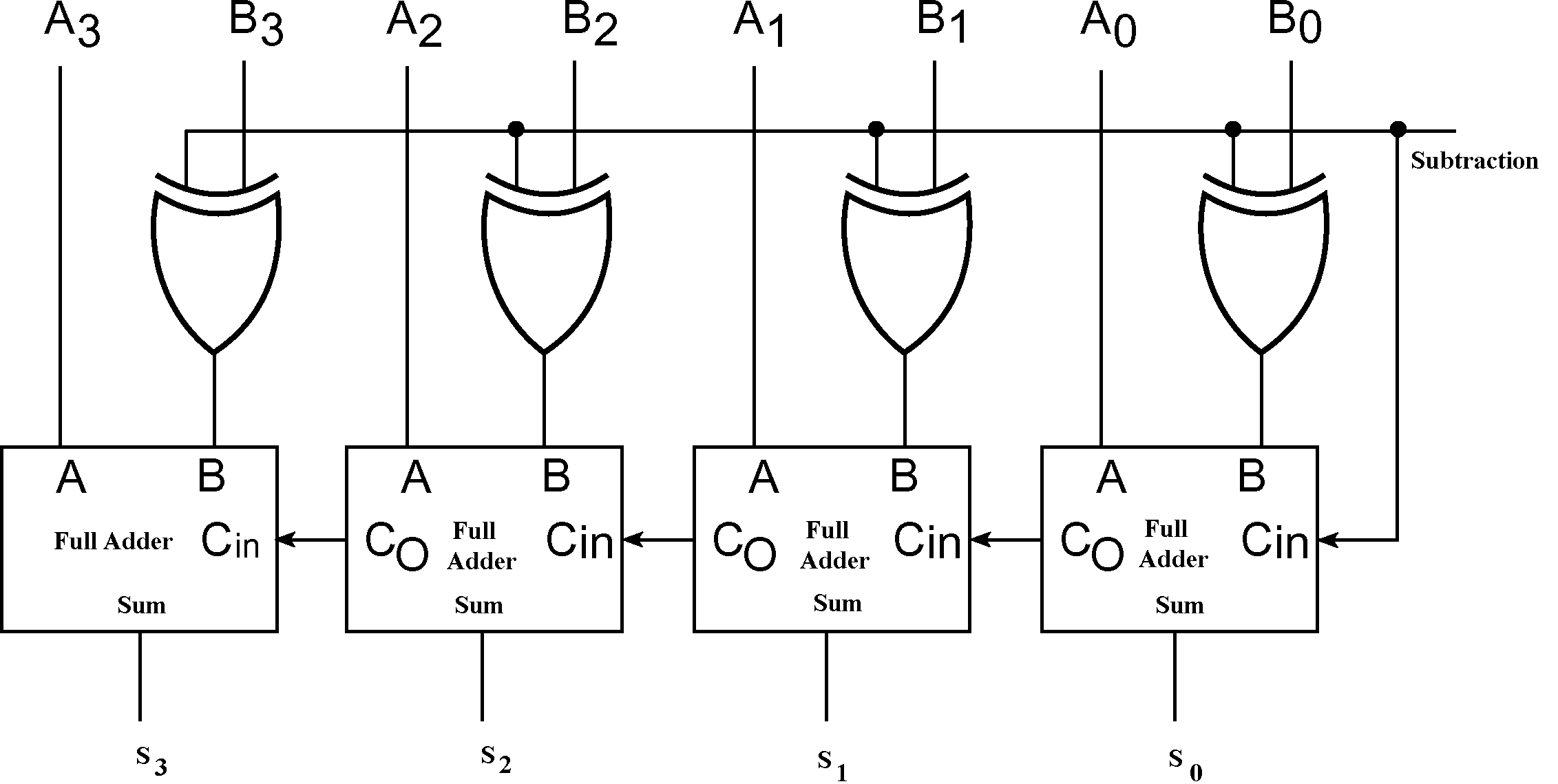
4 Bit Adder Circuit Diagram - Caret X Digital